Electron-Beam Lithography Training
This is an introduction to electron-beam lithography with the Vistec/Raith EBPG at Yale University. You can already tell that this sequence of web pages is simply a dump of a PowerPoint presentation. These extra notes at the bottom are things I might have said while you sleep during the class. Off we go!
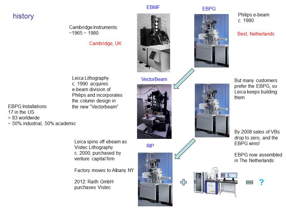
History
The EBPG has a long history, stretching back to the 1960s. This particular e-beam system was first built by Philips (in the Netherlands), then was bought out by Cambridge Instruments (UK), which morphed into Leica Lithography, spun off as Vistec (and moved to the US), and now finally acquired by Raith (Germany). The EBPG is currently built in the Netherlands, where it began long ago. Throughout all this turmoil the EBPG has survived mostly due to customer loyalty and the commitment of a few key people in manufacturing and support.
Intro- Page 3
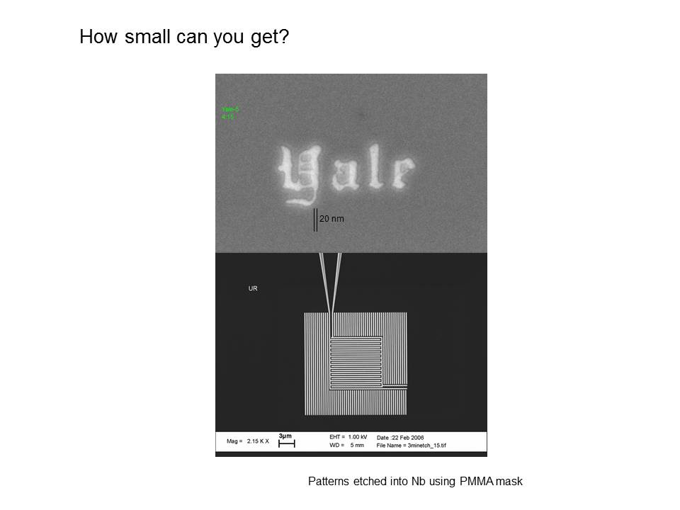
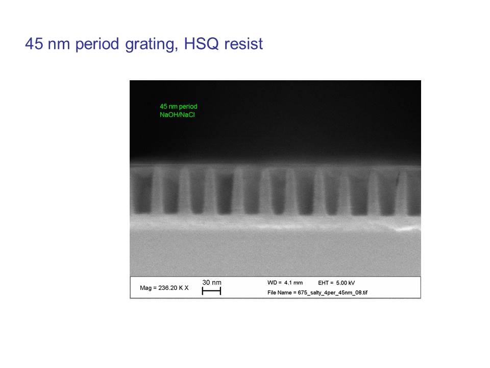
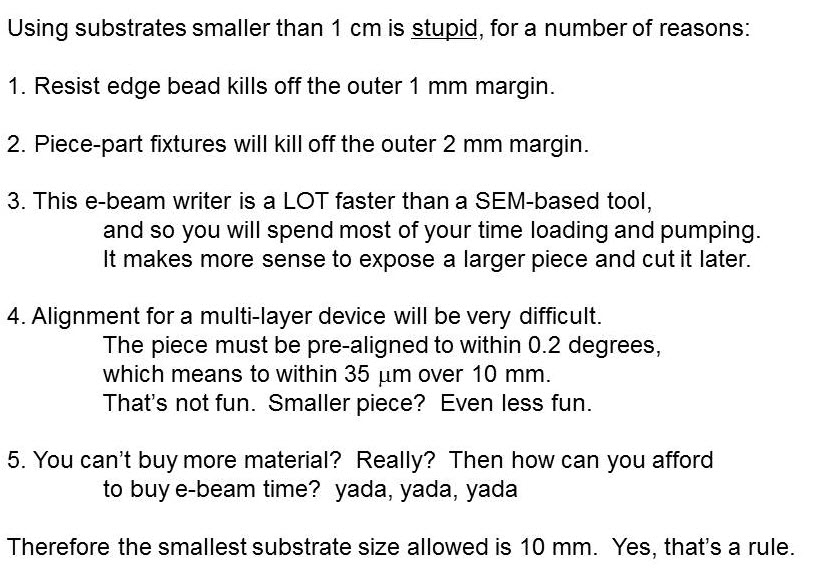
The first question is always “how small”, and the answer is about 10 nm if you work at it.
Intro Page 4
Lovely. But this is just thin resist, not a device.
Intro Page 5
People have written smaller features, using scanning electron microscopes (SEMs) converted for beam writing. So why not use a converted SEM instead of the big, fancy EBPG? Let’s consider that question.
A SEM is almost an e-beam writer
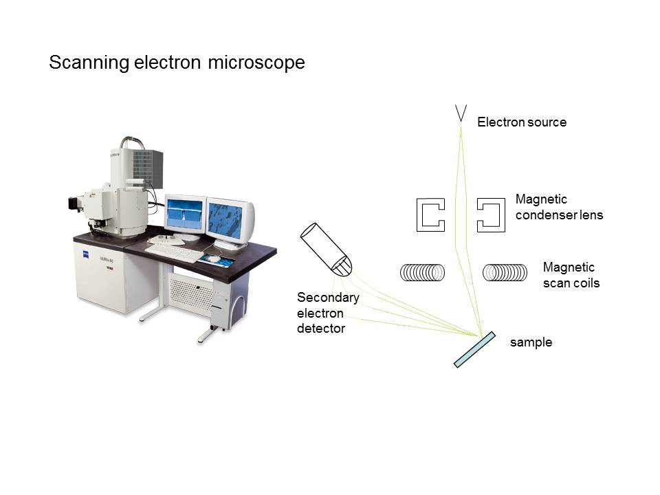
This is a high-resolution Zeiss scanning electron microscope (SEM). It is the same one used in the low-end conversion kits sold by Raith, and it’s the same one that has generated linewidths less than 8 nm. The diagram shows a simplified view of the electron column. The scan coils are built for low noise, and so have very low bandwidth.
SEM Page 2
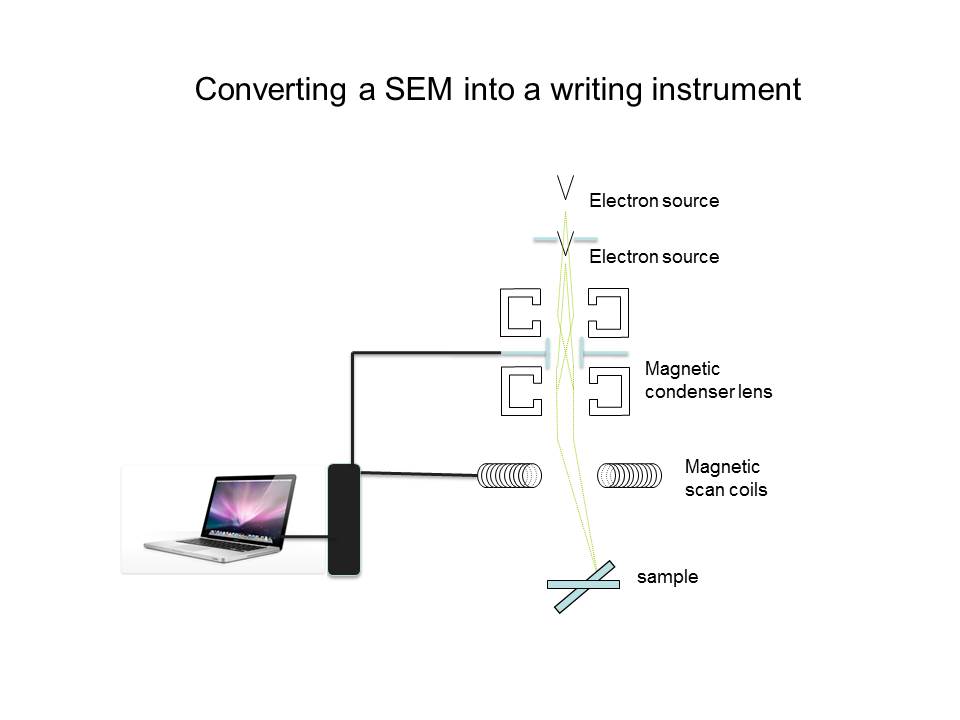
To convert a SEM into a writing instrument, one must insert a “beam blanker” in the column. The scan coils are controlled with a computer. Actually, the Zeiss SEM shown in the previous slide does not have two condenser lenses, and so the beam blanker has to go right inside the electron gun. (But that’s just trivia.)
SEM Page 3
 NEXT>
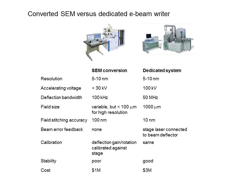
NEXT>There are three big differences between a SEM and a big beam writer: speed, accuracy, and automation. The low bandwidth of SEM deflectors allows the instrument to write fine lines, but the catch is that those lines may not land where you want them. It’s like an uncertainty principle: low noise and low bandwidth lead to a larger uncertainty in placement, since the beam takes longer to settle after deflection. The SEM also has problems building large patterns out of small writing fields. If a pattern is built up from multiple exposure fields then the SEM will stitch those fields together poorly, compared to the dedicated system. Ease of use is a more subjective matter, but most people agree that the big systems are easier to use. They are certainly a lot faster, especially since they include automated calibration routines.
SEM Page 4
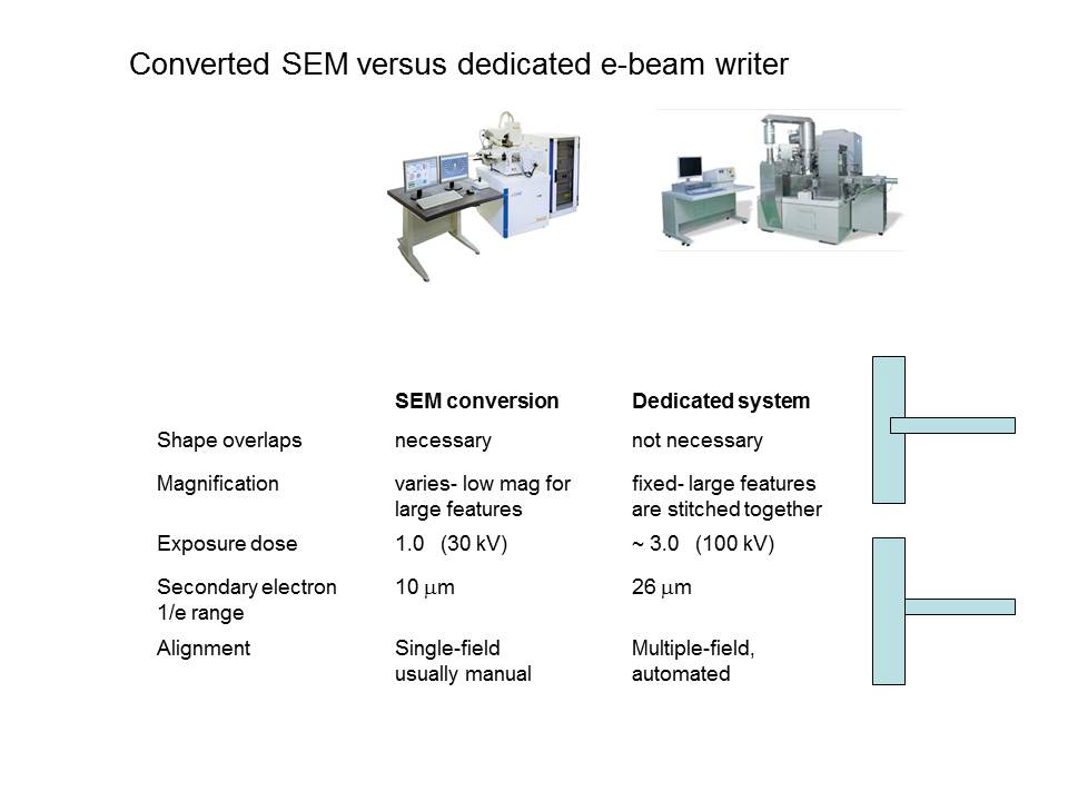
Because of the low bandwidth deflectors, SEM writers often require patterns to include overlaps, so that wires will not contain accidental gaps. Also, users often find it necessary to specify the order in which shapes are written, to minimize hysteresis effects. Really. Is that something you want to think about? (By the way, the e-beam system shown on the right is a JEOL 6300, which is a popular instrument in the US, but it’s not the one we have at Yale.) The table above states that the 100 kV system will require roughly 3 times the dose of electrons, but the high-voltage electron source is also three times brighter. In other words, lower resist sensitivity is offset by higher current. (“brightness” is the current in a given spot size)
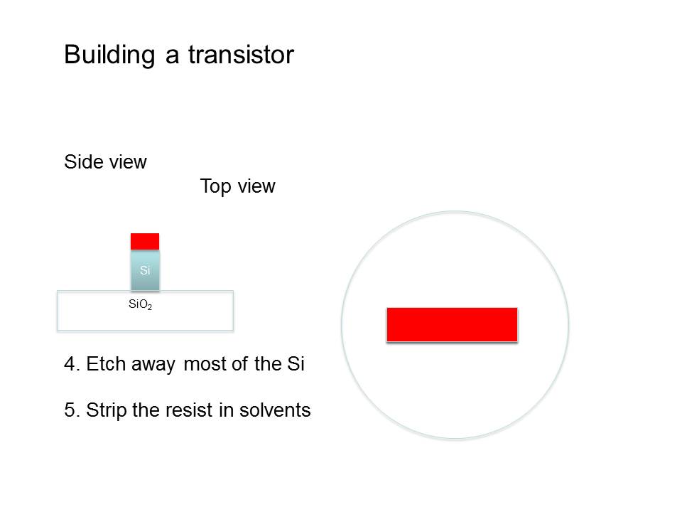
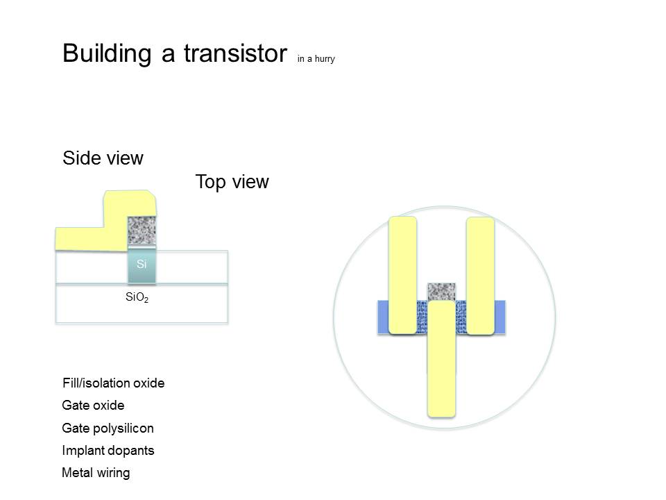
Device Example: a transistor
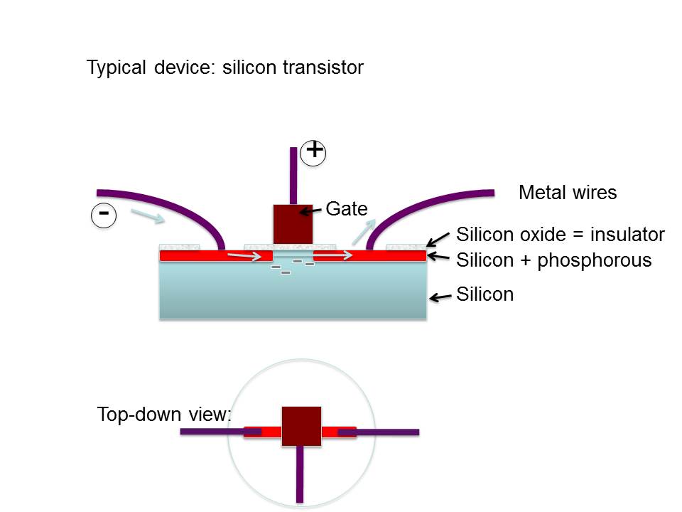
As an example, let’s consider the design of a field-effect transistor (FET). If you don’t know how a FET works, then pay close attention, because you don’t want to look like an idiot after getting out of graduate school. When the gate is charged positively, electrons are attracted toward it. These electrons change the region under the gate into a conductor, allowing current to pass from (let’s say) the left wire to the right. Or right to left - whatever. When the gate is not charged then the electrons under the gate dissipate and the transistor turns off. This is a typical device to build with electron-beam lithography, and it makes a nice example of how to organize your computer-aided design (CAD).
Transistor Page 2
Transistor Page 3
Pattern Transfer
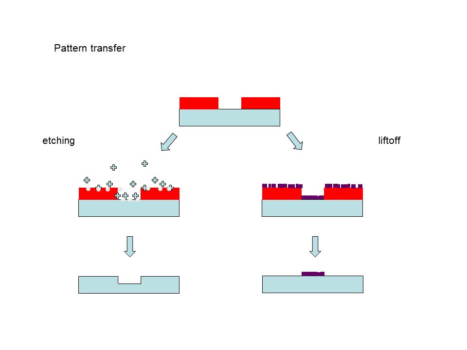
Pattern Transfer Page 2
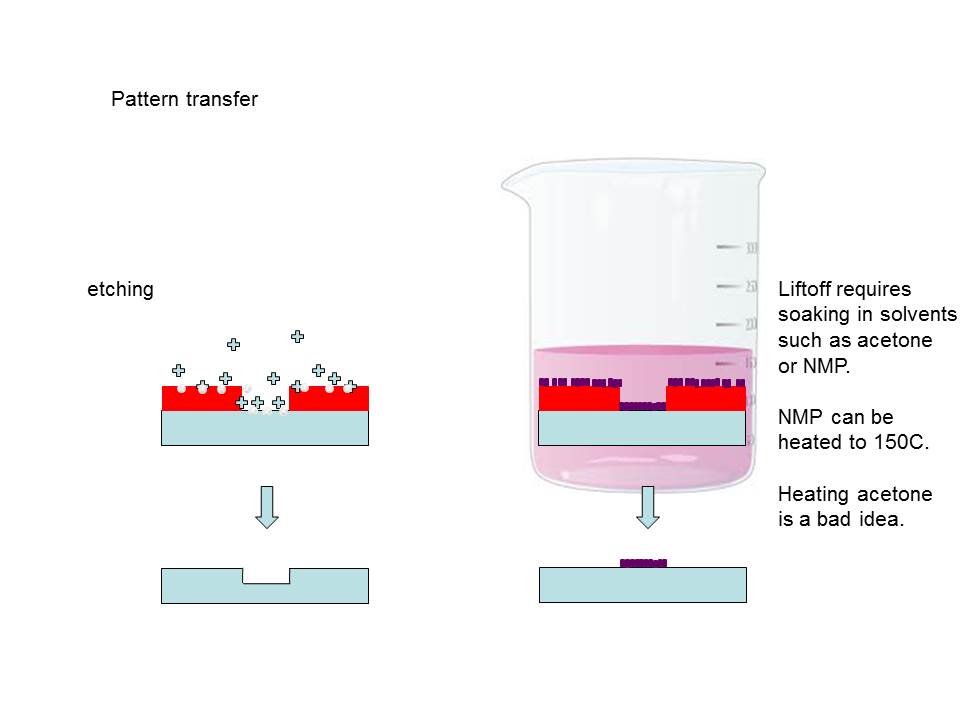
Liftoff of metal wires requires soaking the wafer in solvents to “lift off” the unwanted metal. This is a common technique in research, because it is so simple, but liftoff is not usually used in production since there are more reliable and less messy ways of patterning wires. Acetone is a common solvent used for dissolving resist, and it becomes more effective if you heat it. But it also becomes explosive if you heat it! So if someone tells you to boil the acetone, tell them no- that’s foolish and unsafe. Instead, use warm NMP, which can be heated up to 150C without becoming dangerously explosive. (If you heat NMP above 200C it becomes acidic. Isn’t that strange?)
Pattern Transfer Page 3
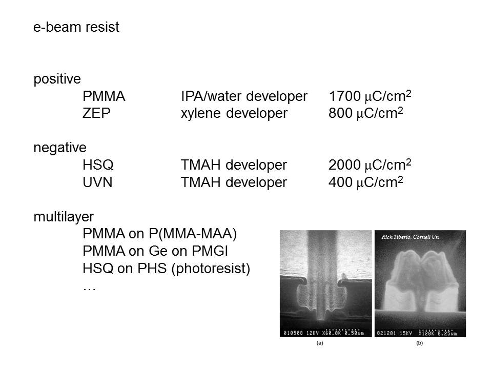
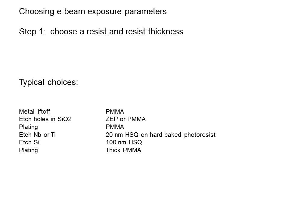
In electron-beam lithography you have a limited selection of resists. The positive resists PMMA and ZEP are polymers that are broken up by electron irradiation. After exposure, the smaller bits dissolve faster in the “developer”. This is a very simple contrast mechanism; there isn’t any complex chemistry as you find in photoresist. (There are more complicated chemically amplified e-beam resists, but they are way too fussy and not worth the effort.)
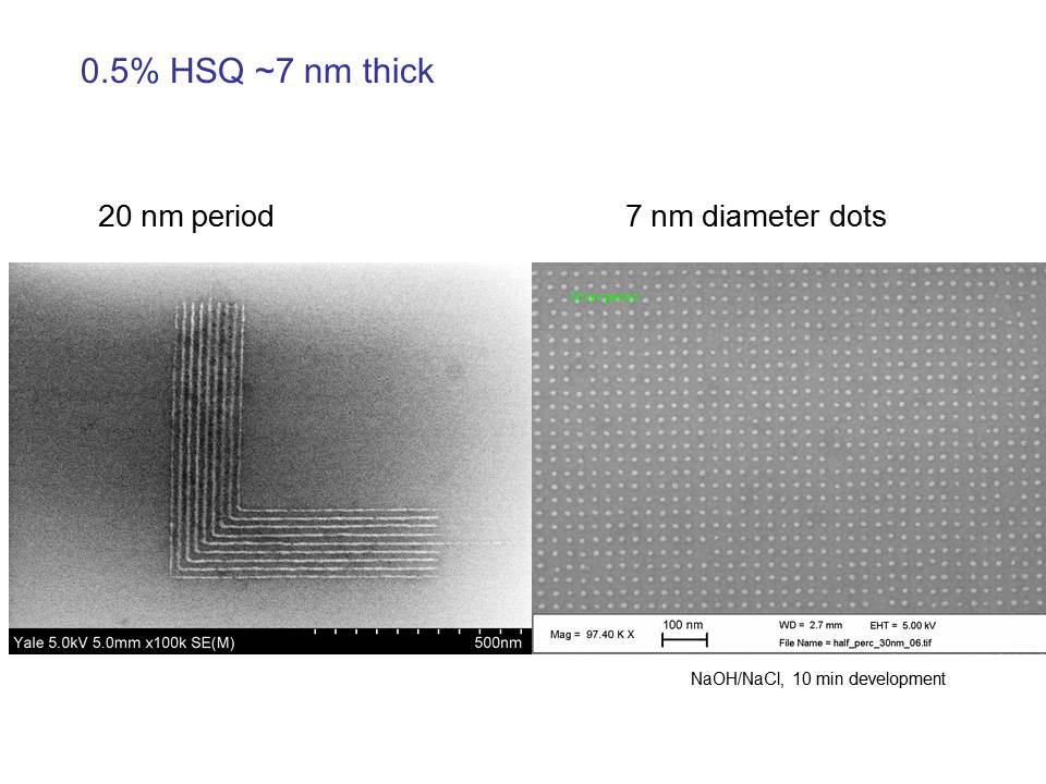
The negative resist HSQ contains monomers which are crosslinked by the electron beam. The unexposed regions wash away in developer. UVN and ma-N are two other negative resists, but are far more difficult to use. For no apparent reason, ma-N negative resist has become more popular than UVN. Both have at best 50 nm resolution, and both use chemical amplification to induce crosslinking. HSQ has the best resolution of any e-beam resist, in the range below 8 nm.
Multilayer resist systems usually involve PMMA and the copolymer P(MMA-MAA). The copolymer is more sensitive to electron exposure, and so we typically put a layer of copolymer UNDER a layer of PMMA to form a large undercut resist profile. A large undercut is handy for doing metal liftoff.
YINQE provides PMMA, ZEP, HSQ and copolymer. We do not stock UVN and ma-N, and so if you want to use one of these then you’re on your own. ZEP and HSQ are quite expensive, and so we have to charge extra for those.
Pattern Transfer Page 4

Pick your developer. The best developer for PMMA is cold IPA+water (3:1), which we keep in a dedicated tank in the YINQE lab. If someone tells you to use MIBK-IPA mixtures instead, they are very much out of date. IPA-water is better in every way: higher resolution, less residue, less swelling, higher aspect ratio, lower toxicity, and lower cost.
ZEP can be developed in a wide assortment of chemicals, depending on your needs. There is a tradeoff between sensitivity (speed) and resolution. If you need to expose large features quickly, then you can use hexyl acetate as the developer. But most people use cold xylene to develop ZEP, since they need the best resolution.
When developing HSQ, there is a tradeoff between resolution and stress. That’s right: strong developers are used for the highest resolution, and these developers require very high electron doses. High doses shrink the resist more than low doses, leading to more stress in the resist film. Depending on the pattern, HSQ might peel off, crack, or “unzip” due to stress. That’s why people will use patterns of dots and short lines to show the highest resolution. For more practical applications we use a weaker developer. Around here we usually develop HSQ in MF312 (which is 0.54N TMAH) for 4 minutes.
Pattern Transfer Page 5
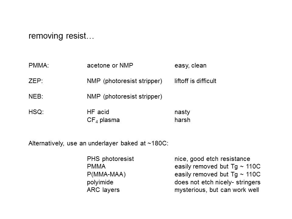
You might not want to think about it now, but at some point you’ll have to remove the resist from your wafer. The liftoff process dissolves resist in solvents, so that’s simple. If PMMA or ZEP is used as an etch mask, then you can remove the remaining resist simply by programming an oxygen etch step in the same plasma etcher. Just hit it with an oxygen plasma after (say) chlorine or fluorine. (Note that a low-bias barrel etcher will not do. You need a bit of bias to break up the polymer.)
Removing HSQ can be difficult, since it does not etch at all in oxygen. HSQ is a low-density silicon oxide, and so it will etch readily in fluorine plasmas or in hydrofluoric acid. If your device is incompatible with those etchants, then you could put a sacrificial polymer layer under the HSQ. A thin layer of PMMA or photoresist will allow the HSQ to be stripped in solvents.
Pattern Transfer Page 6
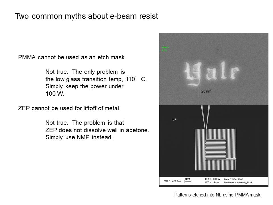
Our colleagues to the north seem to think that PMMA cannot be used as an etch mask. They are badly misinformed! Just keep the plasma power low (<= 100W) to prevent the resist from flowing. ZEP is a somewhat better etch barrier than PMMA, but only by 20% to 30%. That’s not very substantial, so you should be skeptical of exaggerated claims about ZEP. PMMA and ZEP are actually very similar polymers, and so you would not expect them to be terribly different as etch masks.
Proximity Effect
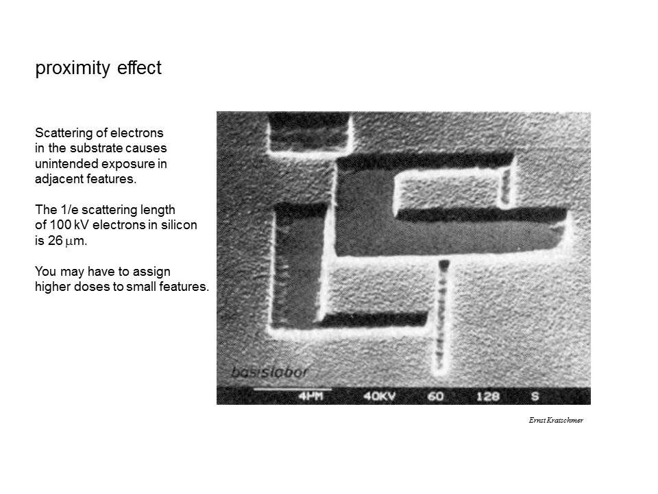
This is a classic picture (from Ernst Kratschmer) showing how large features can be fully exposed while small features are underexposed. It’s a very old picture, and somewhat of an exaggeration, but you get the point: If this pattern were exposed at a higher dose, then the small features would develop properly while the large features bloom out and increase in size. These days we are using 100kV electrons and the effects are much more subtle. For example, if you are writing a 300um wide grating, then the lines at the edges will get about 10% lower dose than features in the middle. If you don’t care about the edges, then don’t worry about it! Are you worried? Ok, then let’s consider a few common solutions.
Proximity Effect Page 2
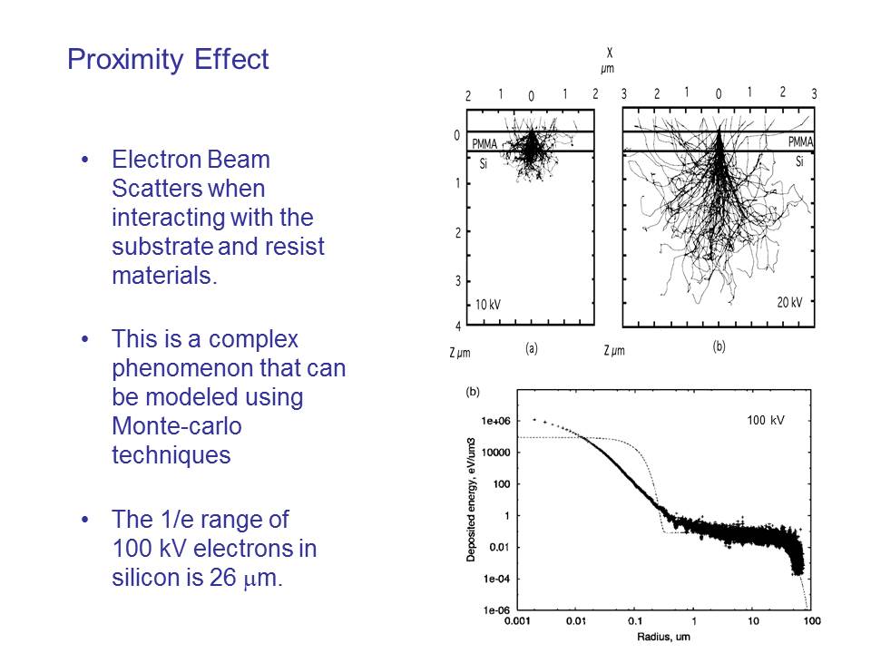
Secondary electrons generated and scattered in the substrate contribute to the dose of other nearby features. How close is close? A 100 kV beam of electrons will scatter in silicon to a range around 26 um (the 1/e range that is). You might think that life would be better at low voltage, but it isn’t. What counts is the ratio of primary electrons to secondary electrons. This ratio is higher at high voltage. Well, that’s not exactly true. When the voltage is below 2 kV or so then the electrons will not even penetrate to the substrate, so at low voltage there is no proximity effect at all! Do you think low voltage e-beam is a good idea? Ha ha: no. We leave it as AN EXERCISE FOR YOU to explain why low voltage lithography is a terrible idea.

Proximity Effect Page 4
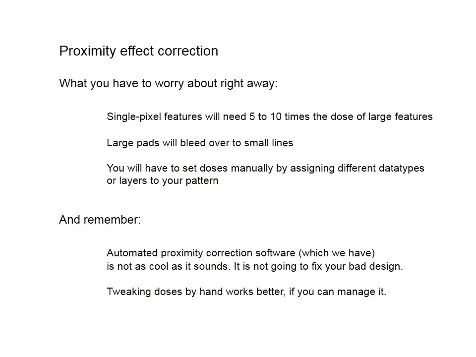
You really do not need to worry about the proximity effect right now, but be aware that we have software which will automatically assign doses to shapes so that exposures will come out more even. Proximity effect correction software sounds nifty, but it helps with only a very narrow class of problems.
E-beam parameters
E-beam parameters Page 2
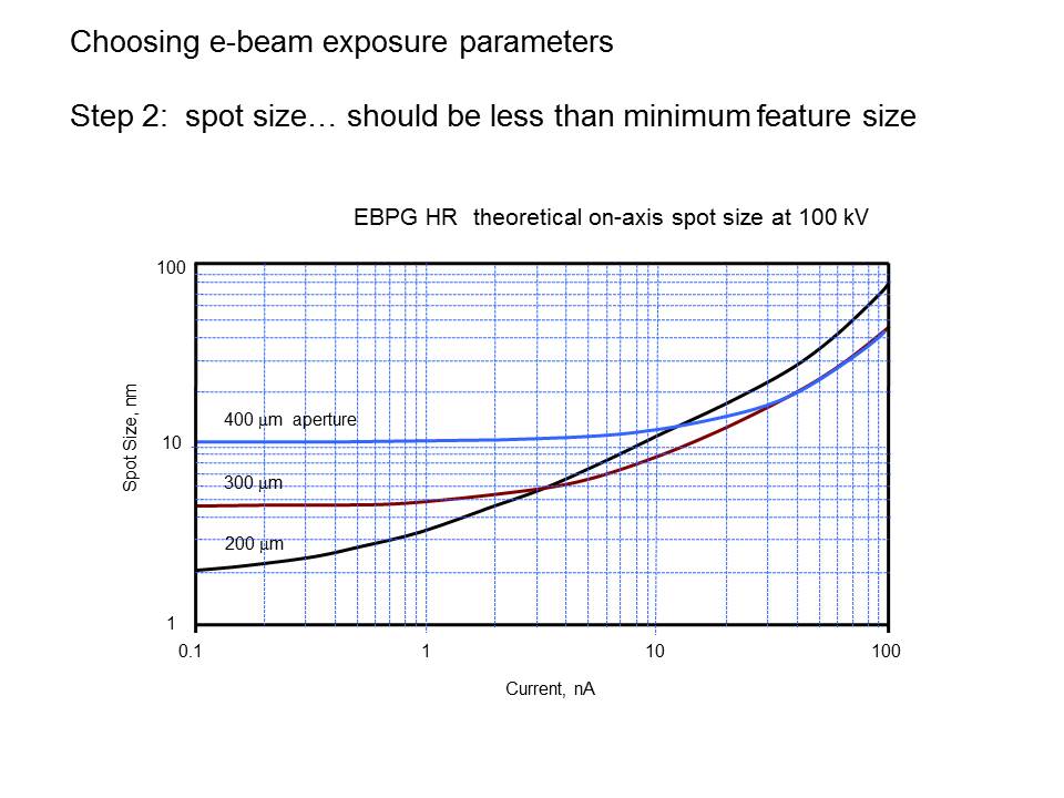
For example, if you want 20nm wide lines you should use a spot size no larger than about 5nm. According to this plot, you could choose the 200um aperture at 3 nA, or you could choose the 300um aperture at 1 nA. So the 200 um aperture is the better choice. If you set up an exposure job that calls for different currents and different apertures, the system will switch to them automatically. Yes: it will even switch apertures automatically!
E-beam parameters Page 3
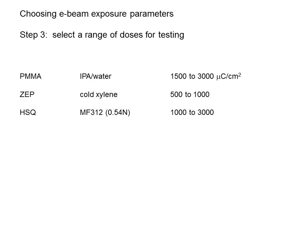
Your first run should always be a dose test. Choose a range of doses that goes from too low to too high. Then expose your pattern (or part of it) a number of times using different doses. The best dose will depend on the pattern, the substrate, the developer and to some extent on the pattern transfer technique. It’s not like using a paper printer; some testing and tweaking is always required.
E-beam parameters Page 4
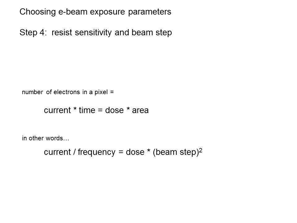
What do we mean by “area”? If you plug in the area of your pattern, then the calculated time will be the total exposure time. If you plug in the area for one pixel then the time will be the “dwell time” for one pixel. The dwell time is the inverse of the clock frequency. The highest clock frequency is 50 MHz. This constrains the exposure current and the beam stepping distance.
E-beam parameters Page 5
The beam step size is the effective pixel size, even if the beam spot is larger or smaller than this number. Use the beam step size when calculating the dose delivered to one pixel. The beam step size is always a multiple of the least significant bit of the deflector DAC. If you don’t know what a digital-to-analog converter (DAC) is, then look it up. One bit on the EBPG’s DAC deflects the beam 1 nm. We have a 20 bit DAC, so… WHAT IS THE MAXIMUM DEFLECTION?
E-beam parameters Page 6

E-beam parameters Page 7
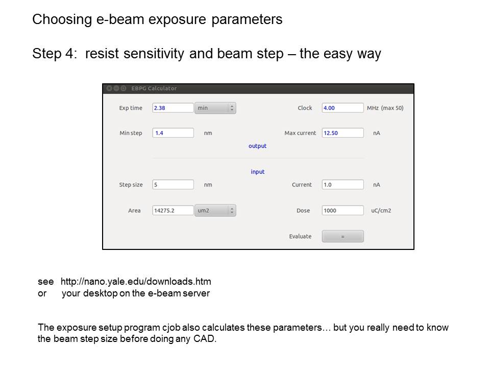
That’s right: you can use this handy dandy parameter calculator. The calculator can be found on the e-beam server desktop. Use the parameter calculator to answer THESE QUESTIONS.
EBPG hardware tour
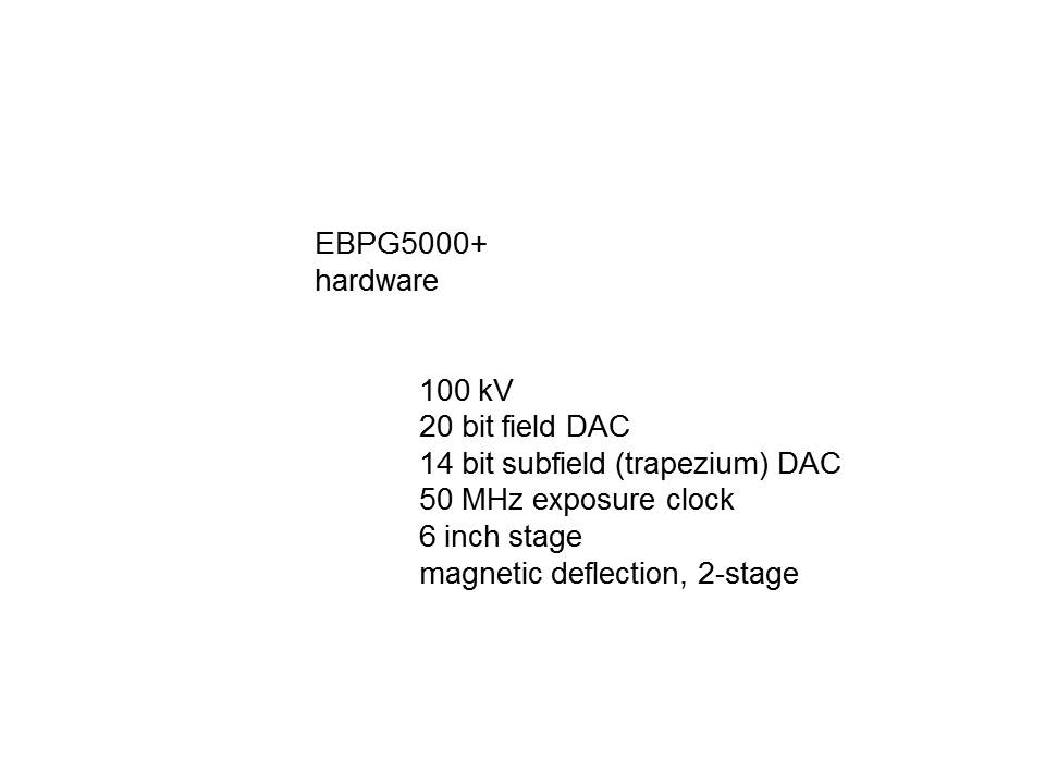
EBPG hardware tour Page 1
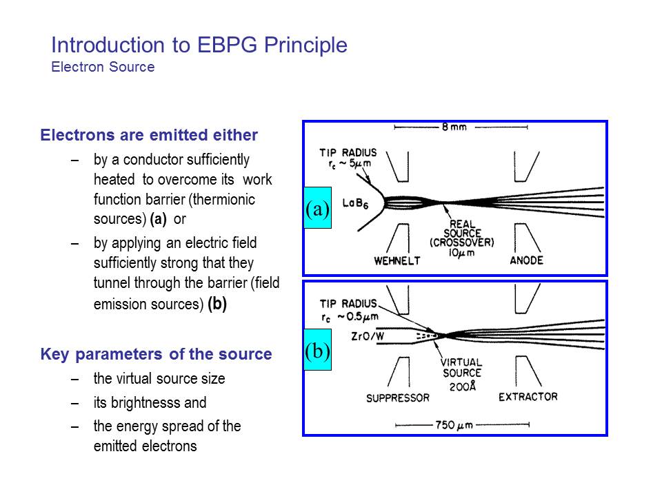
Our EBPG uses the emitter shown in (b), and these days so does every other e-beam system. This electron source is called a “field emitter” because a high field at the tip induces electrons to tunnel out of the metal. It is called a “thermal field emitter” because the tungsten pin is kept hot to keep it clean. Also, the heater allows ZrO to flow down to the sharp end, where it lowers the work function of the metal.
EBPG hardware tour Page 2
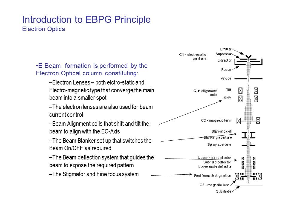
There are three major lenses. The topmost is an electrostatic lens on the electron gun. The second is a magnetic lens which forms a crossover of the beam inside the blanker. The blanker uses an electric field to turn the beam on and off, and because it sits at a beam crossover, there is no image shift when the beam is blanked. The third lens focuses the beam to a spot on the substrate.
EBPG hardware tour Page 3
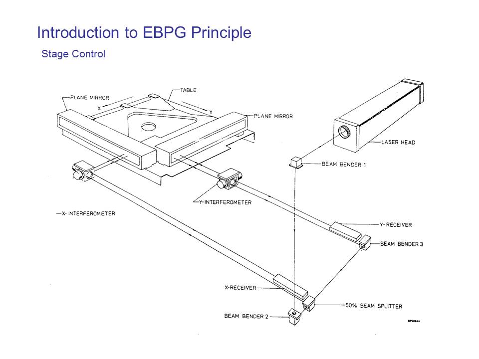
The stage is controlled with a laser interferometer, which is so accurate that it is used to calibrate beam deflection and distortion. You might think that it works by counting fringes, but no. It actually works just like the State Trooper’s radar gun, measuring a Doppler shift as the stage moves. By integrating the speed of the stage, this interferometer can measure the stage position to less than a nanometer. (It’s really quite interesting how the laser works. The He-Ne laser contains a magnet which splits the optical line with the Zeeman effect. The split frequencies are detected with a mixer that generates a difference signal in the gigahertz range. This is a low enough frequency to be measured with common electronics which measure the frequency shift as the stage moves.)
EBPG hardware tour Page 4
EBPG hardware tour Page 5
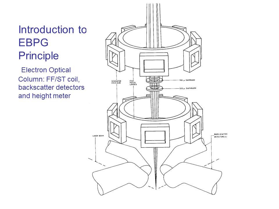
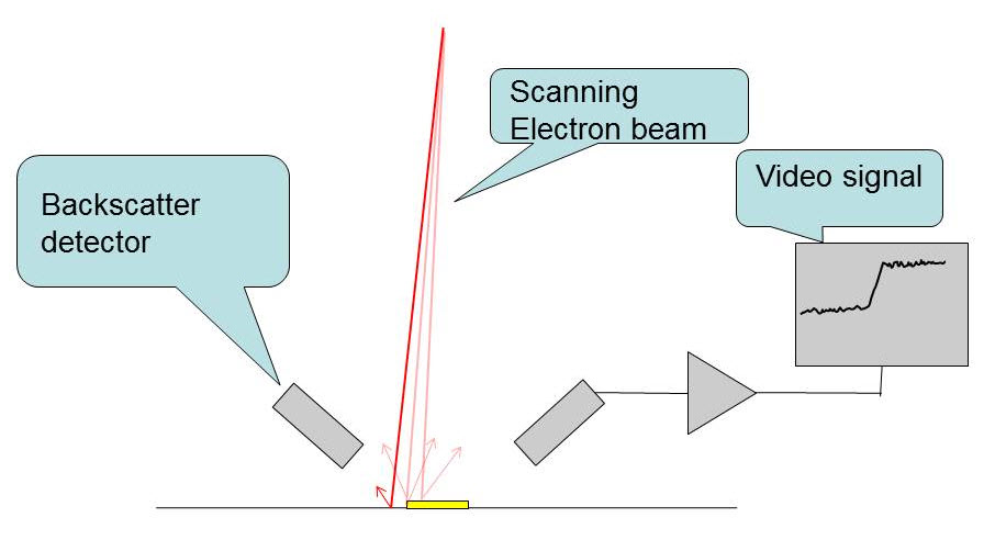
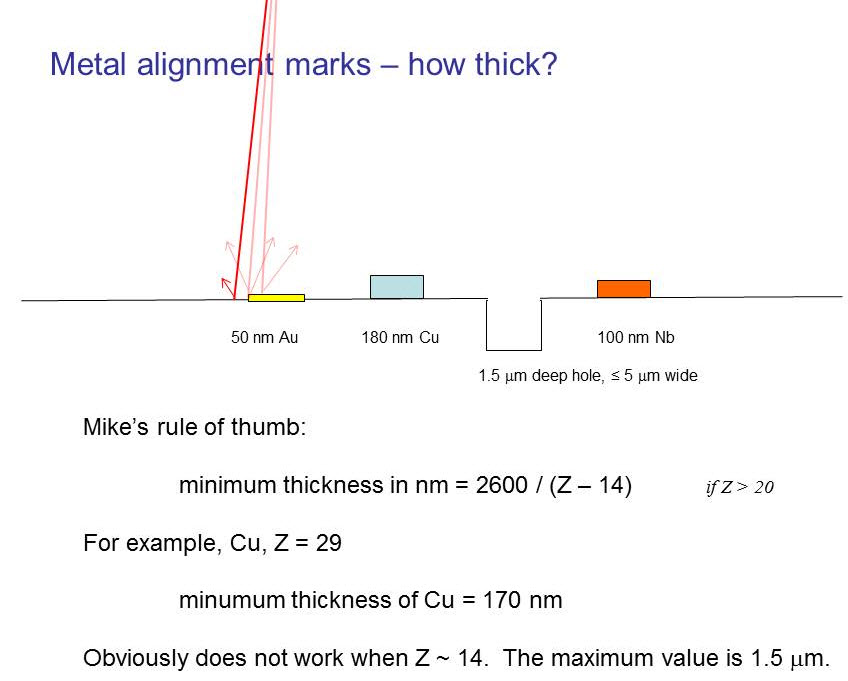
Secondary electrons from the substrate are picked up with a set of four scintillators on light-pipes on photomultiplier tubes. These are just like the detectors in scanning electron microscopes, except that there is no bias drawing in the scattered electrons. A bias would distort the writing field. Unfortunately the lack of bias makes the detectors inefficient, and so the system does not make a good electron microscope. Of course, it operates at 100kV, so that would make a terrible SEM in any case! It might surprise you to find that things easily seen in a SEM can be nearly invisible in the EBPG. That’s why the choice of materials for alignment marks is so critical and restricted.
Other e-beam writing systems use silicon diodes as detectors. These are not as fast as photomultiplier tubes, but they are more efficient at collecting the signal.
EBPG hardware tour Page 6
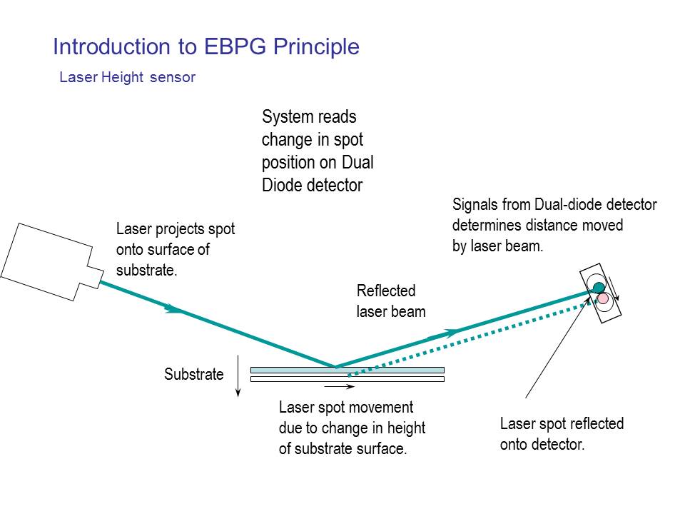
Another laser in the system measures the sample height. The height is measured on each exposure field, after which the EBPG corrects the focus and field size. This measurement and correction takes just a few milliseconds. You might wonder how the height measurement is converted to a focus correction. Well I’m going to tell you anyway. Think of the plot of focus versus height-signal: it’s more or less a straight line, and the slope never changes. The y-intercept of that straight line is determined while calibrating the system before an exposure. During calibration, the EBPG automatically focuses on a reference mark, and then measures the height with the laser sensor. This sets the offset; that is, the y-intercept of focus versus height.
EBPG hardware tour Page 7
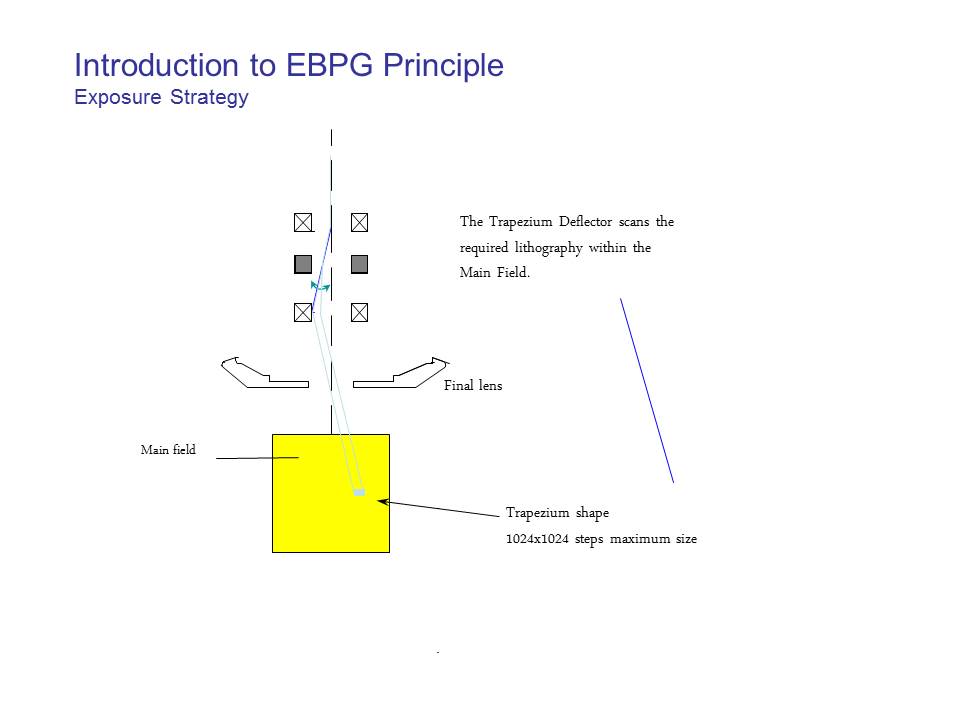
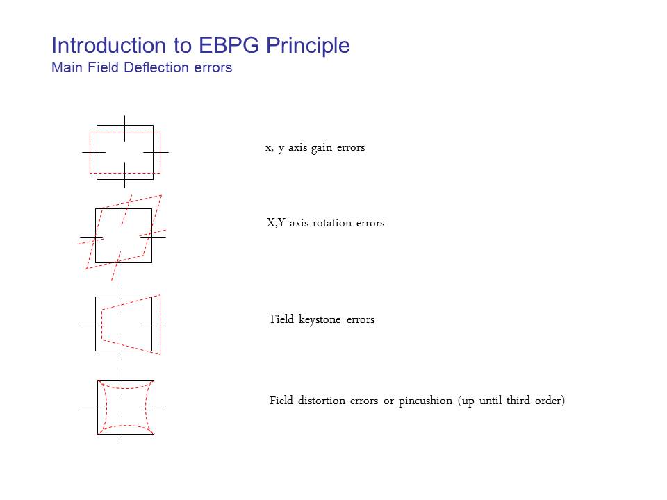
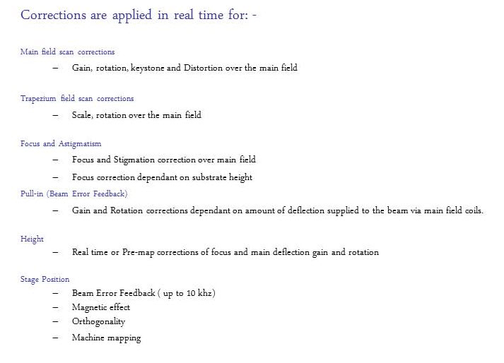
There are two sets of deflection magnets: the (slow) main field deflector and the (fast) trapezium deflector. The origin of each shape is first set with the main deflector, and then that shape is filled in using the fast trapezium deflector. Each deflector is driven by a separate DAC: the main field has a 20 bit DAC and the trapezium deflector has a 14 bit DAC. (You don’t know what a DAC is? Look it up.)
Introduction to EBPG Principle

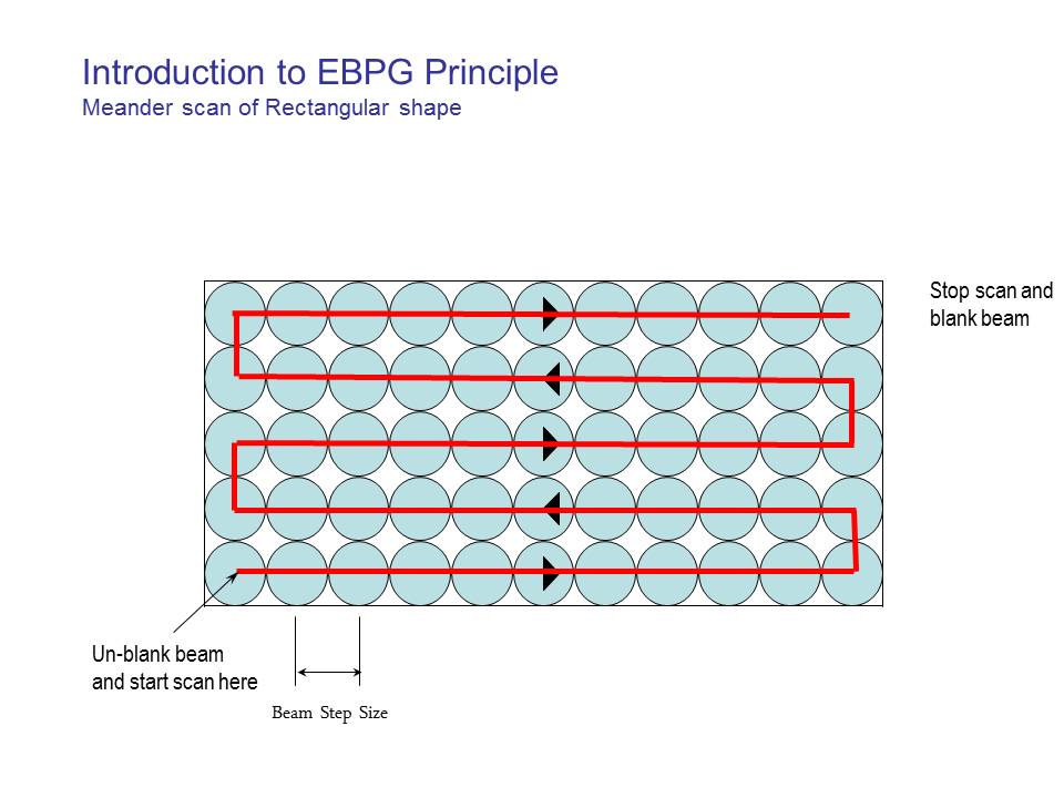
The pattern is split into fields (or “blocks”) that are smaller than the maximum beam deflection. After writing one field, the sample stage must move. Patterns are further broken down into “subfields” which are typically tens of microns in size. A 20-bit DAC deflects the beam to the origin of each subfield. Shapes inside a subfield are further broken down into small trapezoids that can be filled in (or “painted”) with a high-speed 14 bit DAC. Most e-beam writers use a rigid grid of subfields. The EBPG’s pattern generator can use a fixed grid of subfields, or it can use a 20-bit “main field” deflection for each shape. However, most pattern conversion programs (such as Genisys Beamer or Synopsis CATS) do not give you this choice. Your patterns will always be chopped into a rigid grid of subfields.
Introduction to EBPG Principle- page 2
Introduction to EBPG Principle- page 3
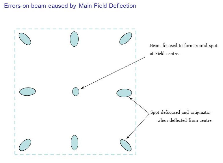

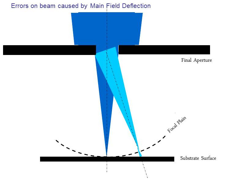
Substrate Height Effect
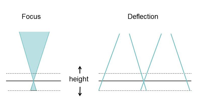
As the substrate height varies, the system must correct both focus and field size. The depth of focus is actually quite large– several microns. Correcting the field size is more critical, since this determines field stitching accuracy. You can see now why smaller field block sizes lead to smaller stitching errors.
On the EBPG you should keep the block size less than 700 um so that field stitching errors will be less than 50 nm. The maximum block size is equal to the maximum field, 1 mm. But it would be a mistake to use such a large deflection.
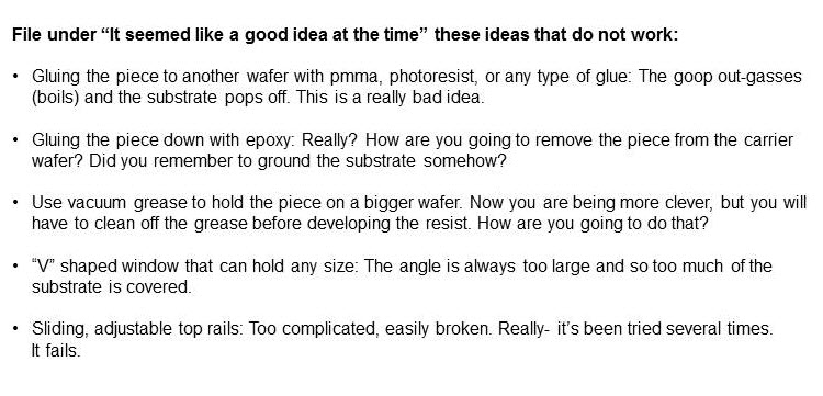
EBPG Sample Holders
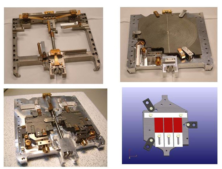
Top left: holder for 5 inch mask plates. Top right: wafer holder. Bottom left: two two-inch wafers (we do not have this one). Bottom right: piece holder. This is a bottom-reference piece holder which we do not have at Yale. This holder requires manual trimming to level the substrate and to move it into the correct plane. The next slide shows a better design.
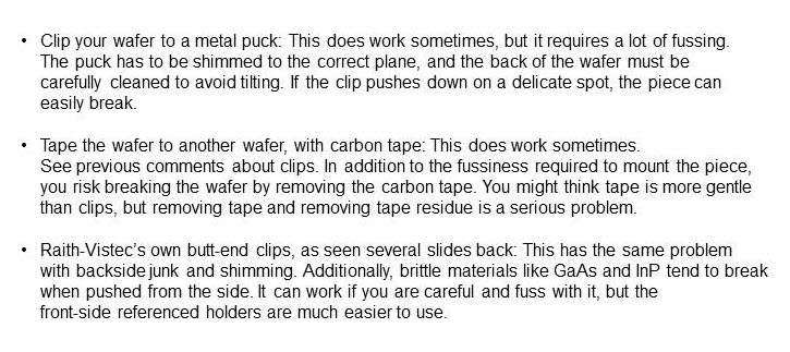
Adapters for small pieces
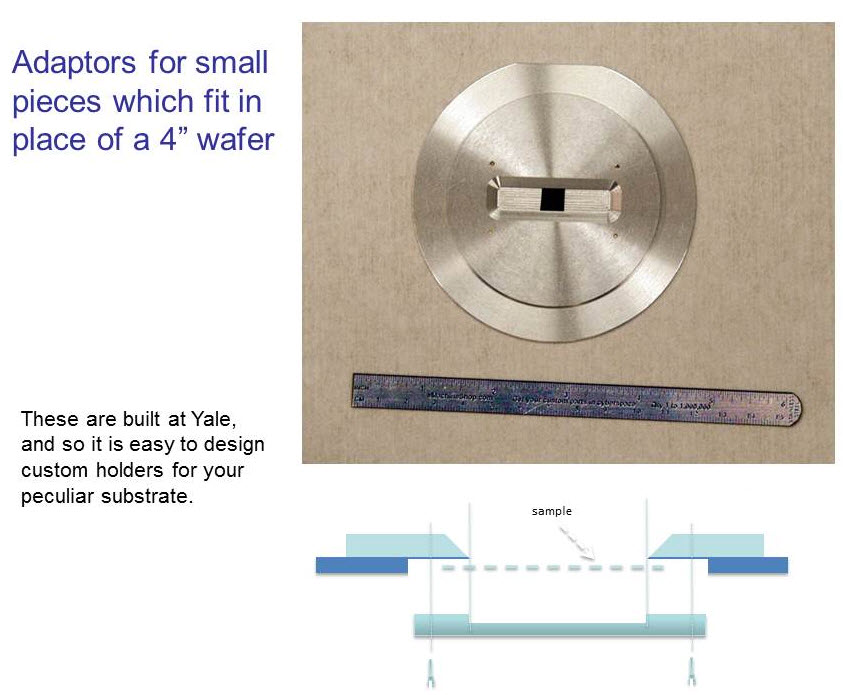
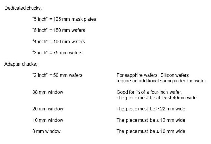
The piece holders we use at Yale are top-surface referenced. In other words, the top of the substrate is pushed onto the correct focus plane. Residual dirt or resist on the back of the substrate will not change the position of the front surface. It is much easier to mount pieces in this holder, as long as the substrate is at least 2mm wider than the widow width. See next slide for a list of window sizes. If you have a substrate that does not fit any of these, it is easy to have the machine shop build a new one.
This top-referenced holder was first developed at Cornell University (for a JEOL system) and later used at IBM and many other laboratories.
Substrates & Holders
A word to the wise
Alignment marks
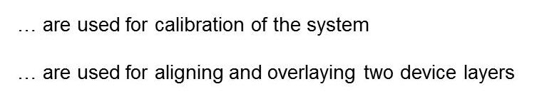
Marker Block & Faraday Cup
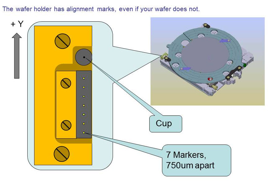
Gold marks on the reference block allow the system to calibrate beam deflection and distortion. The Faraday cup is used for measuring beam current. It is simply a hole from which secondary electrons cannot escape. Do you know who Michael Faraday was? Better look him up, and then ANSWER THIS QUESTION. The positions of markers and Faraday cups are stored in the EBPG, so you need only indicate which sample chuck you are using.
What is a marker?
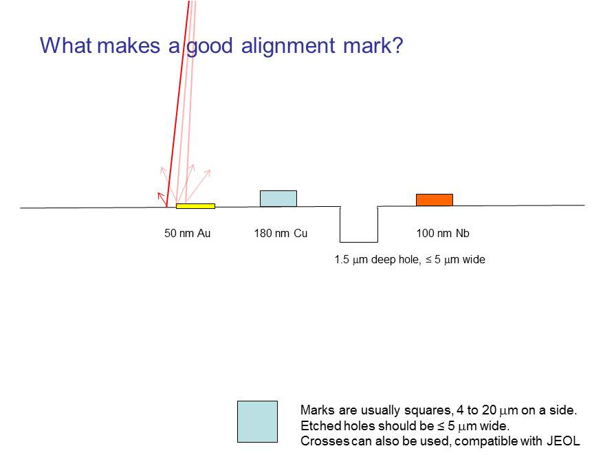
What else can be used as an alignment mark?
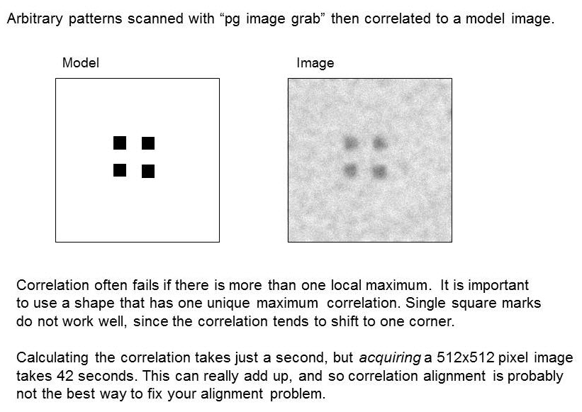
Strange alignment mark example: silicon nitride windows
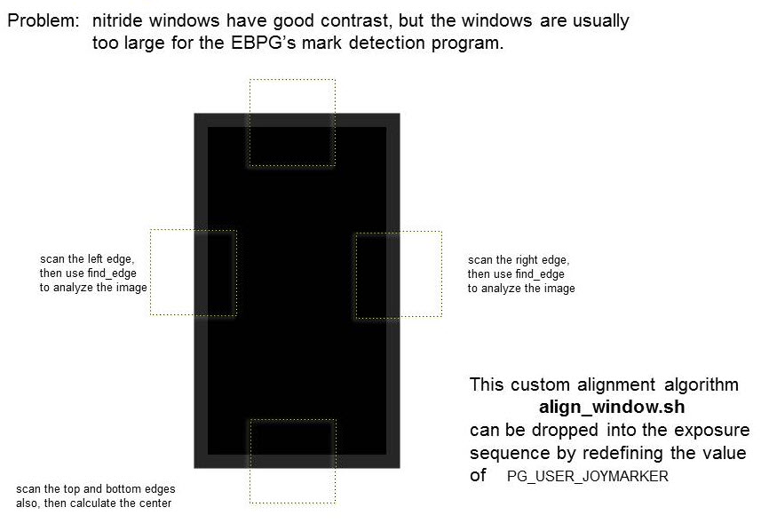
Here is a case where both standard alignment and correlation alignment fail. Silicon nitride windows provide high contrast “marks” but these windows are usually larger than 100 um, the maximum mark size on the EBPG. Instead of using standard mark detection, we collect images of each side, then analyze these images with “find_edge”. The sequence is defined in a script (align_window.sh) that you can plug into an exposure job.
Alternatively, the EBPG has an imprecise alignment mode in which the operator simply points to a location to indicate where the “mark” is. This type of marker is called “joy” for the use of a virtual “joystick”. You don’t know what a joystick is? Don’t worry, it won’t be on the test.
This is the test: THE CRUEL WORLD OF ALIGNMENT MARKS. Yes, you have to answer these questions.
Computer Aided Design
Computer aided design (CAD) programs help you design patterns, then produce output in a standard interchange format. Those CAD files can then be converted to a machine-specific format for (say) e-beam patterning. Many CAD programs produce the output format GDSII, also known as “GDS”. This is the most common file standard for electron-beam lithography and photolithography. A more modern format is “Oasis”, which few people use even though it’s probably fine. Good CAD programs which produce valid GDS format include
Layout, from Juspertor UG (we have a site license for this)
Design Workshop
LEdit, from Tanner
These are not free. A simple free CAD program that might fulfill modest needs is
Free CAD programs to avoid include
Kik
Vem
Magic
The CAD tools from Cadence are fantastic for designing integrated circuits, but are not so great at simple geometrical editing. Try your best to avoid Cadence. Common, general-purpose CAD programs such as AutoCAD and DesignCAD can also be used for e-beam lithography, but their output format is a problem. AutoCAD and DesignCAD produce DXF format, for which there are various non-standard interpretations. Lack of standardization is a good reason to avoid these programs. On the other hand, DesignCAD does have a nice facility for designing around photos, so that might be a reason to suffer with compatibility problems.
Some people write their own programs for generating patterns, or use a combination of manual design and algorithmic design. Writing such programs is easy when you use the GDS libraries for C, Python, or Matlab. Alternatively, a pattern-generating program could spit out the simple text format CIF, which can be read into the CAD programs listed above. Beware: Some CAD programs have internal ‘macro’ languages which are tempting, but such captive programs are very slow and very non-portable. The common term for these macros is “paramatrized cells” or “p-cells”. Macro systems are designed to trap you into one particular CAD program, so don’t be fooled.
Much more information about CAD can be found in the Layout CAD Tutorial.
Next, we will look at the big picture; that is, the overall work flow from design to exposure.
CAD design
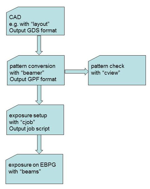
Starting at the top, you will want to work through the Layout CAD Tutorial. Layout (and other CAD programs) produce GDS format pattern files. It is possible to use other pattern formats, such as DXF and CIF, but it’s best to stay with GDS since it is the most stable, standardized, and fully functional. GDS is also known as “GDSII” and “Calma”.
