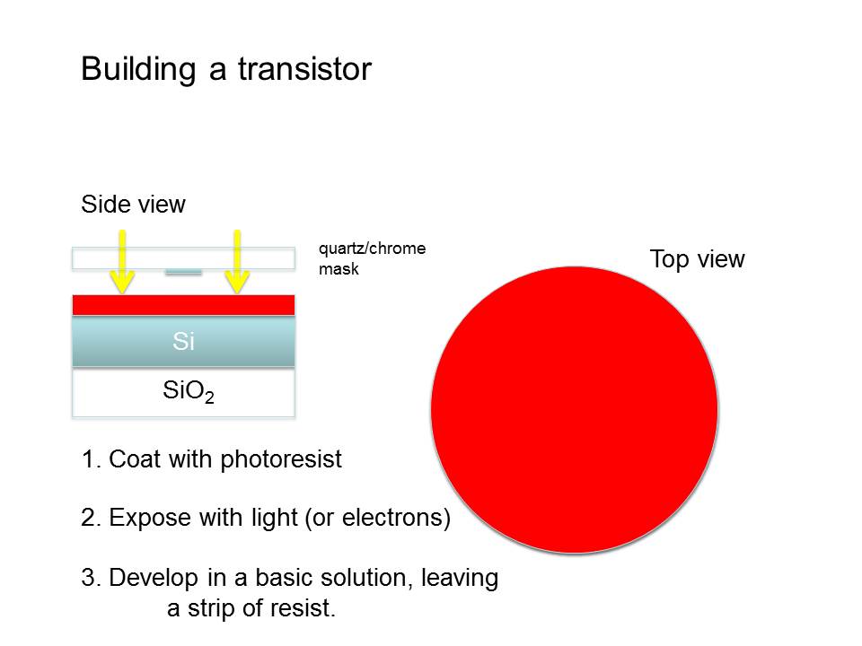
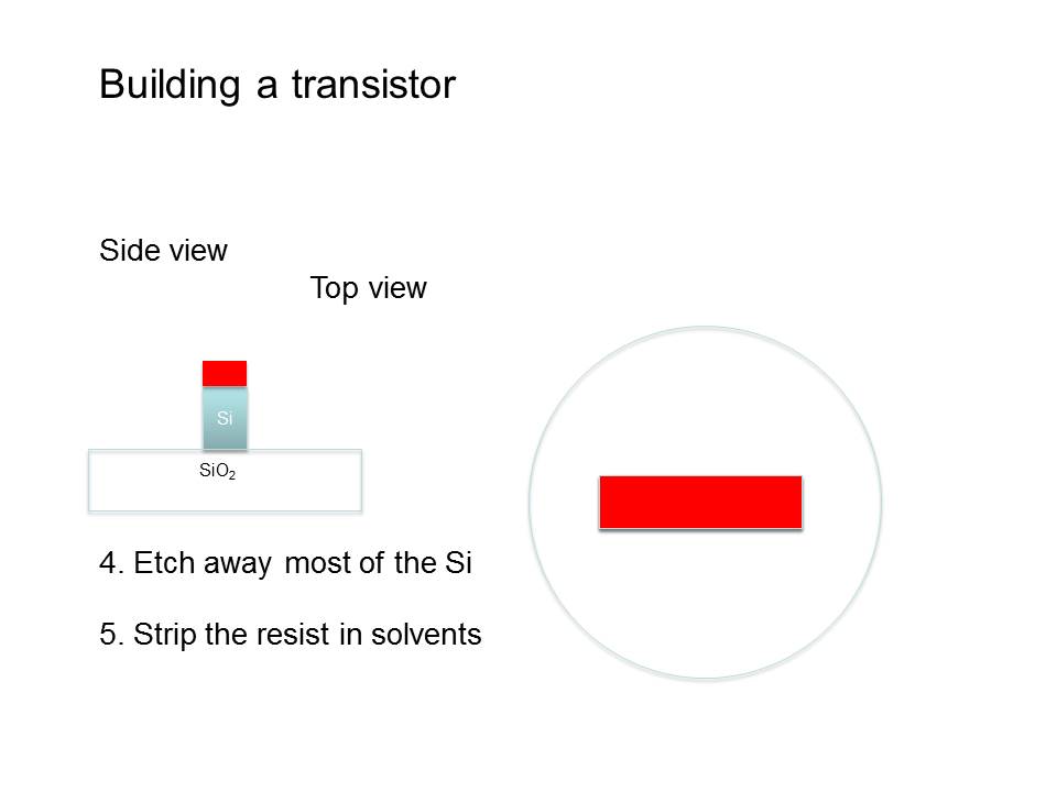
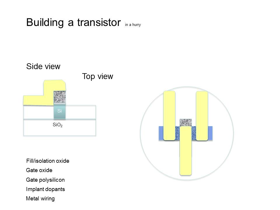
Device Example: a transistor
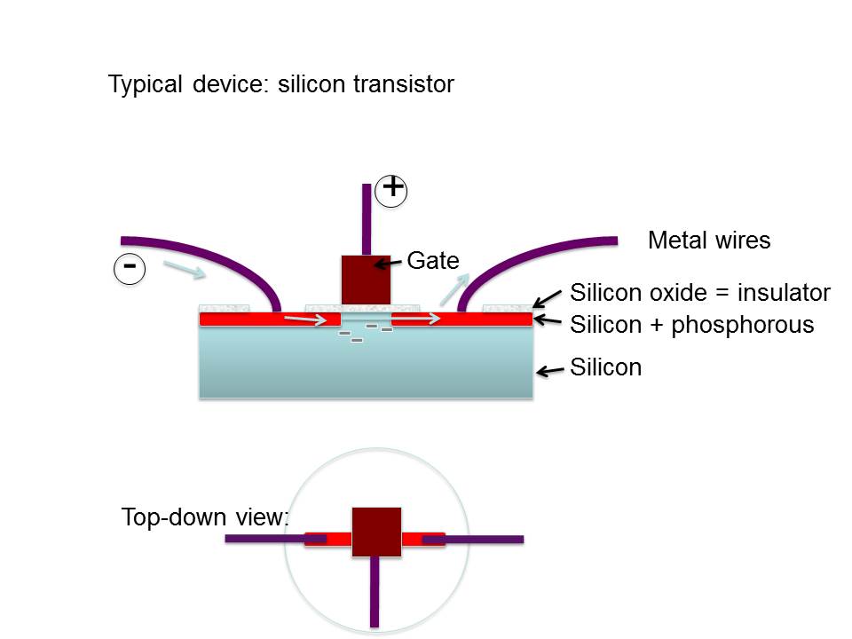
As an example, let’s consider the design of a field-effect transistor (FET). If you don’t know how a FET works, then pay close attention, because you don’t want to look like an idiot after getting out of graduate school. When the gate is charged positively, electrons are attracted toward it. These electrons change the region under the gate into a conductor, allowing current to pass from (let’s say) the left wire to the right. Or right to left - whatever. When the gate is not charged then the electrons under the gate dissipate and the transistor turns off. This is a typical device to build with electron-beam lithography, and it makes a nice example of how to organize your computer-aided design (CAD).