Proximity Effect
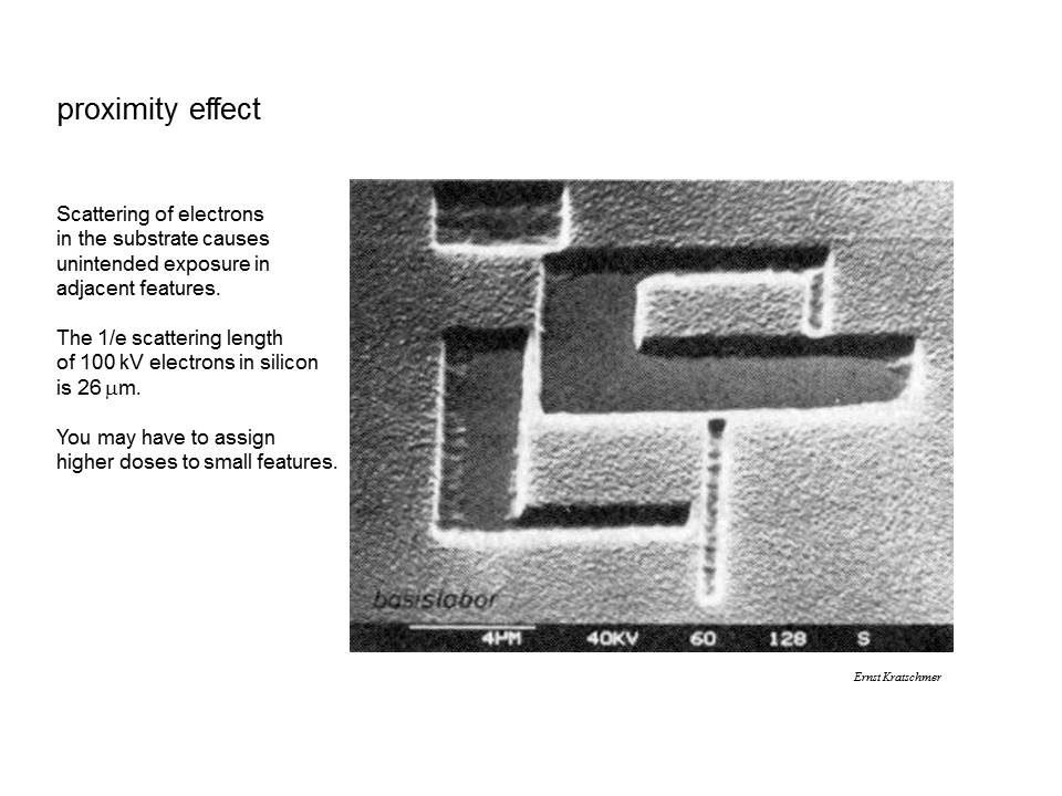
This is a classic picture (from Ernst Kratschmer) showing how large features can be fully exposed while small features are underexposed. It’s a very old picture, and somewhat of an exaggeration, but you get the point: If this pattern were exposed at a higher dose, then the small features would develop properly while the large features bloom out and increase in size. These days we are using 100kV electrons and the effects are much more subtle. For example, if you are writing a 300um wide grating, then the lines at the edges will get about 10% lower dose than features in the middle. If you don’t care about the edges, then don’t worry about it! Are you worried? Ok, then let’s consider a few common solutions.
Proximity Effect Page 2
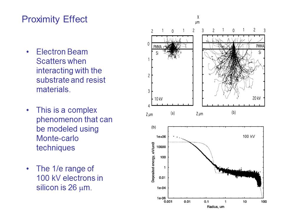
Secondary electrons generated and scattered in the substrate contribute to the dose of other nearby features. How close is close? A 100 kV beam of electrons will scatter in silicon to a range around 26 um (the 1/e range that is). You might think that life would be better at low voltage, but it isn’t. What counts is the ratio of primary electrons to secondary electrons. This ratio is higher at high voltage. Well, that’s not exactly true. When the voltage is below 2 kV or so then the electrons will not even penetrate to the substrate, so at low voltage there is no proximity effect at all! Do you think low voltage e-beam is a good idea? Ha ha: no. We leave it as AN EXERCISE FOR YOU to explain why low voltage lithography is a terrible idea.

Proximity Effect Page 4
You really do not need to worry about the proximity effect right now, but be aware that we have software which will automatically assign doses to shapes so that exposures will come out more even. Proximity effect correction software sounds nifty, but it helps with only a very narrow class of problems.