A SEM is almost an e-beam writer
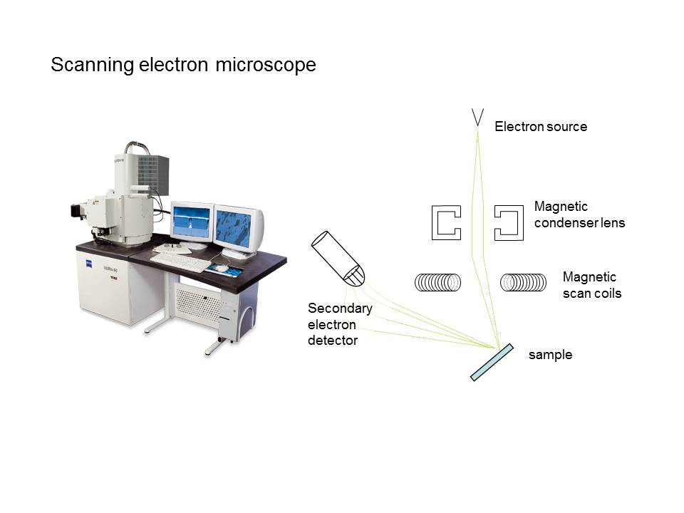
This is a high-resolution Zeiss scanning electron microscope (SEM). It is the same one used in the low-end conversion kits sold by Raith, and it’s the same one that has generated linewidths less than 8 nm. The diagram shows a simplified view of the electron column. The scan coils are built for low noise, and so have very low bandwidth.
SEM Page 2
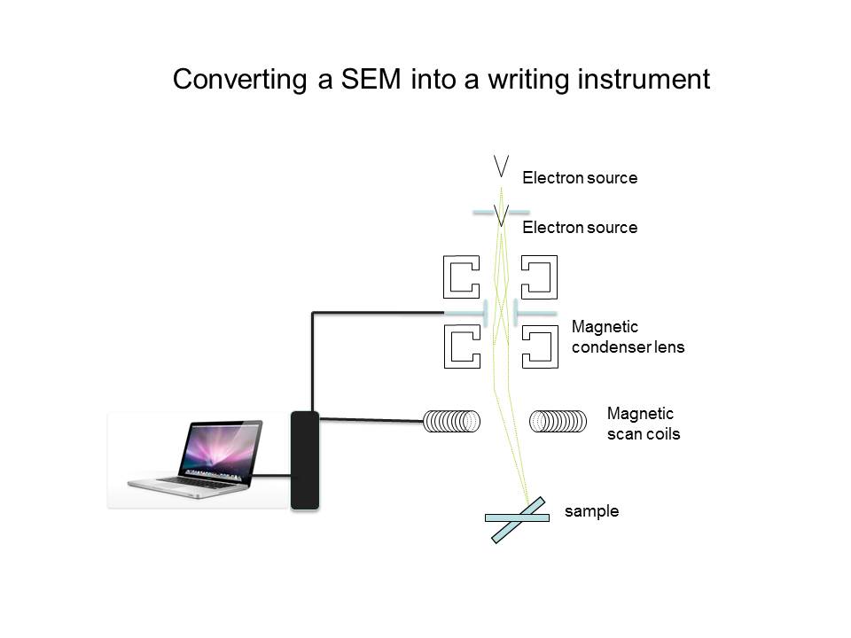
To convert a SEM into a writing instrument, one must insert a “beam blanker” in the column. The scan coils are controlled with a computer. Actually, the Zeiss SEM shown in the previous slide does not have two condenser lenses, and so the beam blanker has to go right inside the electron gun. (But that’s just trivia.)
SEM Page 3
 NEXT>
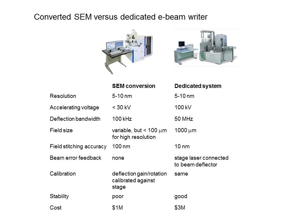
NEXT>There are three big differences between a SEM and a big beam writer: speed, accuracy, and automation. The low bandwidth of SEM deflectors allows the instrument to write fine lines, but the catch is that those lines may not land where you want them. It’s like an uncertainty principle: low noise and low bandwidth lead to a larger uncertainty in placement, since the beam takes longer to settle after deflection. The SEM also has problems building large patterns out of small writing fields. If a pattern is built up from multiple exposure fields then the SEM will stitch those fields together poorly, compared to the dedicated system. Ease of use is a more subjective matter, but most people agree that the big systems are easier to use. They are certainly a lot faster, especially since they include automated calibration routines.
SEM Page 4
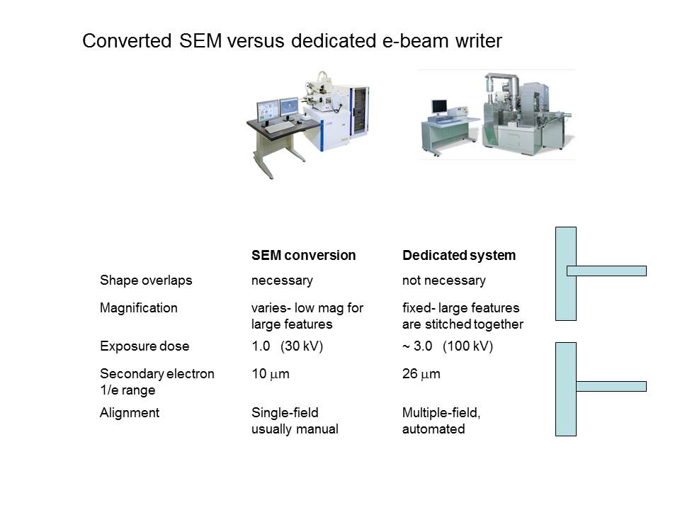
Because of the low bandwidth deflectors, SEM writers often require patterns to include overlaps, so that wires will not contain accidental gaps. Also, users often find it necessary to specify the order in which shapes are written, to minimize hysteresis effects. Really. Is that something you want to think about? (By the way, the e-beam system shown on the right is a JEOL 6300, which is a popular instrument in the US, but it’s not the one we have at Yale.) The table above states that the 100 kV system will require roughly 3 times the dose of electrons, but the high-voltage electron source is also three times brighter. In other words, lower resist sensitivity is offset by higher current. (“brightness” is the current in a given spot size)