Conducting layers for e-beam resist: Gold vs. Aluminum vs. Polymer
tl;dr – Gold is the best. It always has been. Use a 15 nm thick layer; that is, 60 seconds in our Cressington table-top sputter tool.
Long version: they all work, but gold is still the best
When we need to do e-beam lithography with insulating substrates, the most common technique is to deposit a layer of gold on top of the resist. Sputtering gold is fast and reliable, and the gold etches off quickly in a solution of KI. Why should we change? Perhaps you are suddenly paranoid about gold contamination. Perhaps your substrates are too big for the table-top sputtering tool. Perhaps you moved to California where the sputtering tool needs seismic bracing and a municipal building permit.
Ok then, aluminum works well also, and so do various conducting polymers. "DisCharge" polymer is quite convenient, since you just spin it on, let it dry at room temperature, and later wash it off with water.
But before diving into a comparison, let's write down the common wisdom about gold. Everyone knows this:
- For positive resist (PMMA, CSAR, ZEP) use 15 nm of sputtered gold directly on top of the resist. That’s 60 seconds in our little Cressington sputtering tool. Thinner films will be discontinuous.
- After exposure, remove the gold in the KI/water solution known as “TFA”. Rinse in water. If you are using MIBK/IPA for developing PMMA, be very careful to dry off all of the water, since water will drastically change the developer strength. The same thing applies to CSAR developed in other solvents.
- Do not discard the KI gold etchant. It stays good for many years. We have proven this with very tedious tests, so do not create more pollution by throwing away gold etch solution.
- CSAR and ZEP (which are the same) have a rather porous structure, and so the gold etchant can soak through. If your substrate has a metal film, the gold etchant can seep through the resist and attack the metal. In that case, try spinning some water-soluble PSSA on the resist before sputtering gold. Then you can wash off the metal with water. Or use a conducting polymer.
- To use gold on HSQ, first spin on the water soluble polymer PSSA. Bake it at 120C for a minute, and then sputter the gold… or aluminum. The metal will wash right off with water.
Now let's compare gold, aluminum, and the conducting polymer "DisCharge" from Dischem Inc. (We use the "X4" version of DisCharge, which spins to about 100 nm at 3000 rpm.) You might also want to know about the polymer Espacer, but we did not test it because it's too expensive.
Of these three coatings, which is best? Well gold of course, but let's do a fair comparative test.
Peeling metal layers
One disconcerting thing about metal layers is that they peel off the resist if the shape is large or if the dose is very high. Or do they? Optically, we can see dark patches where the metal seems to be gone:
Looks pretty bad, right? But let’s put it in the SEM to get a closer view. The gold has not really peeled away. It is just very rough and cracked. The resist has bubbled under the gold, but the film is still providing a very good conducting layer. Here a SEM image of gold on PMMA, after exposure:
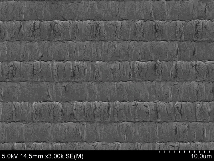
In the SEM at low magnification, 5 kV, the gold film does not display any of the typical signs of charging - dark halos or shifting shadows. The gold has survived spectacularly.
Well, maybe not entirely. These small tears and cracks can act like lightning rods. Charge builds up in the substrate, and then a discharge can occur between the substrate and the cracked metal. It's really spectacular but I don't have a picture! If any of you have seen the craters that occur from this effect, please send me the SEM image. This lightning strike is something that might happen every few chips, in an irregular pattern. You can avoid it by using a lower current or multi-pass writing.
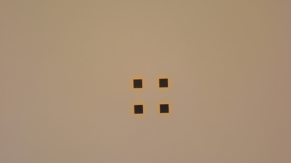
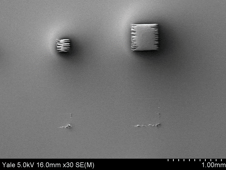
Aluminum seems to peel worse than gold, and when we look at it at 5 kV in a SEM, we really do see telltale signs of charging. Here is a SEM image of aluminum on PMMA (on sapphire) after exposure. There are four squares in this image. The two on the top are charging badly, while the two on the bottom are not. It's hard to see the ones on the bottom.
In this exposure test, we varied the size of the square in the X direction, and varied the dose in the Y direction. By looking at the metal at low magnification, we created a simple chart showing which ones failed and which ones were ok:

The chart is shaded where the aluminum film failed. This exposure was done at 50 nA. The results are worse at 100 nA. The chart for a gold coating is too boring to show here. They all worked! There were no failures at all.
Note that we really had to blast the aluminum to get it to fail. In the range of normal PMMA doses, the aluminum coating was perfectly fine.
The same test for the conducting polymer “DisCharge” shows even better results:

Therefore, we can rank the contestants of the peeling test: #1 Gold, #2 DisCharge, #3 Aluminum. They all work fine in the normal dose range.
Alignment
But that's NOT the whole story! What happens when we zoom into an alignment mark to scan it very intensely? Many of us have seen gold peel up in nasty ways when we do alignment on thick resist (~1um, typically PMMA/copolymer). This did not happen during the tests shown here (with 500nm thick PMMA) but it's definitely a problem when using thicker resist.
In this next test, gold alignment marks on sapphire were coated with 500 nm thick PMMA. Then the PMMA was coated with our three contenders: 15 nm gold, 20 nm aluminum, and 100 nm thick DisCharge polymer. (No, not all at once. We had three wafers for the test.)
In each case, we used the EBPG to align to one of the marks. Five alignments were done at 30 nA, 100kV, then we turned on the beam in "viewing mode" for one minute. Are there signs of failure? The wafers were not developed, but instead were viewed in a SEM at 5 kV to look for charging artifacts.
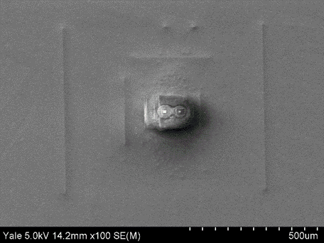
Here is the gold-coated PMMA. You can barely make out the mark. It looks great:
Here is the aluminum-coated PMMA. There is some bubbling, but there is no charging:

After alignment, the DisCharge film shows evidence of charging. The polymer appears to have degraded during the alignment scans. Note the dark shadow on the lower-right side:
Therefore, gold clearly wins the alignment test, and aluminum comes in second place. The DisCharge polymer has broken down, which might cause poor alignment. To be sure about this conclusion, we should measure actual alignment accuracy using alignment marks. But that's a lot of work, so it will have to wait. For now we can only say that the polymer might have a problem when doing alignment.
Conclusion
The clear winner is gold, as expected. Aluminum is not so bad either. DisCharge polymer is ok if you do not need to do any alignments.
Back to the list of tips